УтжАЩљУїЃКБОЭјеОЮЊЙЋвцадЭјеОЃЌВПЗжаХЯЂРДздЭјТчЃЌШчЙћЩцМАЙѓЭјеОЕФжЊЪЖВњШЈЃЌЧыМАЪБЗДРЁЃЌЮвУЧГаХЕЕквЛЪБМфЩОГ§ЃЁ
This website is a public welfare website, part of the information from the Internet, if it involves the intellectual property rights of your website, please timely feedback, we promise to delete the first time.
ЕчЛАTel: 19550540085: QQКХ: 929496072 or гЪЯфEmail: Lng@vip.qq.com
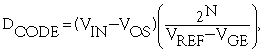
еЊвЊ:SARЃЈж№ДЮБЦНќМФДцЦїЃЉADCЛљзМЕчбЙЖдзЊЛЛОЋЖШЕФгАЯьБШзюГѕЯыЯѓЕФЛЙвЊДѓЁЃЭМ1ЫљЪОЮЊРэЯыКЭДјдівцЮѓВюЕФ3ЮЛADCзЊЛЛЦїЕФДЋЕнЗНГЬЁЃADCЕФДЋЕнЗНГЬЕШгкЃК ЁЁЁЁдкетРяЃЌDCODEЮЊЪ§зжЪфГіДњТыЃЌVINЮЊзЊЛЛЦїЕФЪфШыЕчбЙЃЌVOSЮЊзЊЛЛЦїЦЋжУЕчбЙЃЌVREFЮЊгУгкзЊЛЛЦїЕФЛљзМЕчбЙЃЌN..
|
SARЃЈж№ДЮБЦНќМФДцЦїЃЉADCЛљзМЕчбЙЖдзЊЛЛОЋЖШЕФгАЯьБШзюГѕЯыЯѓЕФЛЙвЊДѓЁЃЭМ1ЫљЪОЮЊРэЯыКЭДјдівцЮѓВюЕФ3ЮЛADCзЊЛЛЦїЕФДЋЕнЗНГЬЁЃADCЕФДЋЕнЗНГЬЕШгкЃК
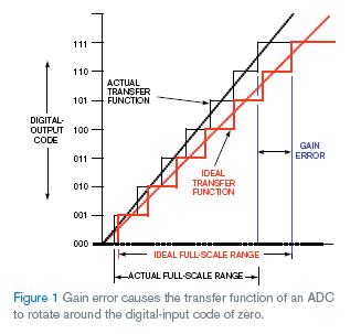
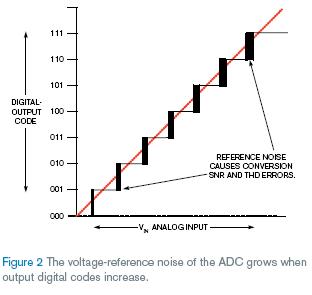
ЁЁЁЁдкетРяЃЌDCODEЮЊЪ§зжЪфГіДњТыЃЌVINЮЊзЊЛЛЦїЕФЪфШыЕчбЙЃЌVOSЮЊзЊЛЛЦїЦЋжУЕчбЙЃЌVREFЮЊгУгкзЊЛЛЦїЕФЛљзМЕчбЙЃЌNЮЊADCЮЛЪ§ЛђADCЗжБцТЪЃЌVGEЮЊADCдівцЮѓВюЁЂЛљзМЪфГіЕчбЙЮѓВюКЭЛљзМЕчбЙдыЩљЕФзлКЯЁЃ ЁЁЁЁШнвзПДЕНЛљзМЕчбЙИјЖЈжЕЖдADCОјЖдОЋЖШЕФгАЯьЁЃЖдИпЗжБцТЪзЊЛЛЦїЃЌЛљзМЕчбЙЦЋжУЮѓВюЭЈГЃБШADCЦЋжУЮѓВюДѓЃЌЬиБ№дкЙ§ЮТЖШзДЬЌЁЃДгДЋЕнЗНГЬвВзЂвтЕНЛљзМЕчбЙЮѓВюЖдНЯИпЪфШыЕчбЙзЊЛЛЦїЕФНсЙћгАЯьИќДѓЁЃ ЁЁЁЁПЩвдгУratiometricЩшМЦМѕаЁADCКЭЛљзМЕчбЙЕФЮѓВюЁЃеташвЊЕчТЗЛђЮЂДІРэЦїаЃзМЫуЗЈжаМгШыЖюЭтЩшБИЁЃМЧзЁаЃзМЫуЗЈашвЊУПИіЕчТЗЕФдівцКЭЦЋжУЬиадЁЃ ЁЁЁЁЛљзМЕчбЙЕФдыЩљЮѓВюЪЧВЛЭЌЕФЮЪЬтЁЃЫќгАЯьзЊЛЛЕФSNRЃЈаХдыБШЃЉКЭTHDЃЈзмаГВЈЪЇецЃЉЁЃЛљзМЕчбЙдыЩљгАЯьЪфШыЕчбЙНЯИпЕФADCзЊЛЛЦїЕФSNRКЭTHDЃЈЭМ2ЃЉЁЃ
ЁЁЁЁШчЙћзЊЛЛЦїдкЛљзМЕчбЙв§НХШБЩйФкВПЛКГхЦїЃЌНЋЛсв§ШыЛђЪфГіЕчСїМтЗхЁЃзЊЛЛЦїдкзЊЛЛЦкМфЪЙгУетаЉЕчСїЮЊФк ЁЁЁЁВЛвЊГЂЪдгУ0VЛђЕиЕФЪфШыЕчбЙВтЪдADCЁЃШчЙћЯЃЭћПДЕНзЊЛЛжаЛљзМЕчбЙдДЕФгАЯьЃЌГЂЪдЪЙгУжБСїШЋЗЖЮЇЪфШыЃЌаХКХЪфШыНЋАяжњПДЕНЯЕЭГЕФЦЕТЪЯьгІЃЈВЮПДЮФЯз1ЃЉЁЃ ЁЁЁЁгЂЮФдЮФЃК ЁЁЁЁADC voltage-reference errors impact full-scale conversions ЁЁЁЁBy Bonnie Baker -- EDN, 11/22/2007 ЁЁЁЁSAR (successive-appoximation-register) analog-to-digital references have more influence on conversion accuracy than you may initially think. Figure 1 shows the transfer function of an ideal 3-bit ADC and the same converter with gain error. The transfer function of an ADC is equal to: ЁЁЁЁwhere DCODE is the digital-output code, VIN is the input voltage to the converter, VOS is the converterЁЏs offset voltage, VREF is the reference voltage applied to the converter, N is the number of ADC bits or the ADC resolution, and VGE is the combined ADC-gain error, reference-output-voltage error, and reference-voltage noise. ЁЁЁЁIt is easy to see how the voltage referenceЁЏs specified value affects the ADCЁЏs absolute accuracy. For high-resolution converters, the reference-offset error is usually greater than the ADC-offset error, particularly over temperature. You will also notice from the transfer function that the reference errors have more influence on the converter results with higher input voltages. ЁЁЁЁYou can reduce the ADC and reference-source errors with a ratiometric design. This scenario may require additional devices in the circuit or a processor/microcontroller-calibration algorithm. Remember that calibration algorithms require gain and offset characterization for each circuit. ЁЁThe referenceЁЏs noise error is a different matter. It affects the SNR (signal-to-noise ratio) and the THD (total harmonic distortion) of a conversion. The reference noise impacts the converterЁЏs SNR and THD at higher ADC input voltages (Figure 2). ЁЁЁЁIf the converter lacks an internal buffer at the reference pin, you will notice incoming or outcoming current spikes. The converter uses these currents during the conversion cycle to charge internal capacitors. This knowl ЁЁЁЁDonЁЏt try to test your ADC with an input voltage of 0V or ground. If you hope to see the effects of your voltage-reference source on your conversions, try to use a dc full-scale input and then a signal input that will help you look at the systemЁЏs frequency response (Reference 1). ЁЁЁЁReference ЁЁЁЁOljaca, Miro and Bill Klein, ЁАImproved Voltage Reference Circuits Maximize Converter Performance,ЁБ Texas Instruments Webinar on Demand. |