��ְ����������վΪ��������վ��������Ϣ�������磬����漰����վ��֪ʶ��Ȩ���뼰ʱ���������dz�ŵ��һʱ��ɾ����
This website is a public welfare website, part of the information from the Internet, if it involves the intellectual property rights of your website, please timely feedback, we promise to delete the first time.
�绰Tel: 19550540085: QQ��: 929496072 or ����Email: Lng@vip.qq.com
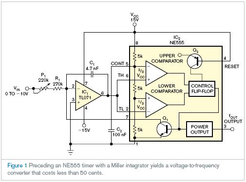
ժҪ:��NE555��ʱ����Miller�����������ɵ�ѹ��Ƶ��ת�������۸����50���֡� ����1971�꣬Signetics����Philips��ǰ������������NE555��ʱ����Ŀǰ������ÿ������������ʮ�ڼ���Ʒ��ͨ����NE555����һЩ���������Թ���۸����50���ֵļ�ѹƵ��ת��������·����NE5..
|
��NE555��ʱ����Miller�����������ɵ�ѹ��Ƶ��ת�������۸����50���֡�
����1971�꣬Signetics����Philips��ǰ������������NE555��ʱ����Ŀǰ������ÿ������������ʮ�ڼ���Ʒ��ͨ����NE555����һЩ���������Թ���۸����50���ֵļ���ѹƵ��ת��������·����NE555��ʱ���ͻ���TL071��Miller��������ͼ1����Ӧ���������ѹΪ0��-10V������0��1000Hz�����Ƶ�ʷ�Χ��C1�ĵ���Ϊ�����ѹ�ĺ�����IC=�CVIN/(P1+R1)��
����C1�ĵ�ѹ�ﵽVCC��2/3ʱ����ʱ�����ڲ��ŵ羧��ܴ�C1�ĵ�ѹ�ص�VCC��1/3���Ƚ����ĵ���ֵ������ѹ��1/3�����ŵ羧��ܹرգ�C1�ٴο�ʼ��硣C1���ʱ��NE555�����Ϊ�ߣ���C1�ŵ�ʱ��NE555�����Ϊ�͡������ѹ��C1���ʱ��ij˻�Ϊ��������Ϊ�ŵ�ʱ��С�ڳ��ʱ�䣬����Ĺ�ʽ���������Ƶ��fOUT~VIN/(P1+R1)��C1��1/3VCC�� ����P1У�����Ƶ�ʺ������ѹ�Ĺ�ϵ����Ϊ�ŵ�ʱ��ԼΪ30µs����ѹƵ��ת���ľ�����Ƶ�ʵ����Ӷ����͡�����趨100H ����Ӣ��ԭ�ģ� ����NE555 timer sparks low-cost voltage-to-frequency converter ����The combination of an NE555 timer and a Miller integrator yields a voltage-to-frequency converter that costs less than 50 cents. ����Gyula Di��szegi and J��nos Nagy, Divelex Ltd, Budapest, Hungary; Edited by Charles H Small and Fran Granville -- EDN, 2/21/2008 ����In 1971, Signetics��later Philips��introduced the NE555 timer, and manufacturers are still producing more than 1 billion of them a year. By adding a few components to the NE555, you can build a simple voltage-to-frequency converter for less than 50 cents. The circuit contains a Miller integrator based on a TL071 along with an NE555 timer (Figure 1). The input voltage in this application ranges from 0 to �C10V, yielding an output-frequency range of 0 to 1000 Hz. The current of C1 is the function of input voltage: IC=�CVIN/(P1+R1). ��As the voltage on C1 reaches two-thirds of VCC, the 555��s internal discharge transistor opens, and the voltage on C1 returns to one-third the voltage of VCC, the lower comparator threshold. At one-third this voltage, the discharge transistor switches off, and C1 again starts charging. The NE555��s output is high while C1 is charging and low while C1 is discharging. The product of the input voltage and the charging time of C1 is constant. Because the discharge time is shorter than the charging time, the following equation results for the output frequency: fOUT~VIN/(P1+R1)��C1��1/3VCC. ����P1 calibrates the relationship between the output frequency and the input voltage. Because the discharge interval is approximately 30 µsec, the accuracy of the voltage-to-frequency conversion decreases as the frequency increases. If you assign 100 Hz to �C1V and 1000 Hz to �C10V, the error of conversion ranges from 0.3 to 3%. If you use P1 to calibrate the output frequency in the middle of the input |