免职声明:本网站为公益性网站,部分信息来自网络,如果涉及贵网站的知识产权,请及时反馈,我们承诺第一时间删除!
This website is a public welfare website, part of the information from the Internet, if it involves the intellectual property rights of your website, please timely feedback, we promise to delete the first time.
电话Tel: 19550540085: QQ号: 929496072 or 邮箱Email: Lng@vip.qq.com
摘要:通过管理芯片和周围空气之间的热传递,维持光耦特性,避免失效。 任何半导体设备的动作依靠其模型温度,这就是为什么电子参数要按照特定温度给出。为维持光耦特性,避免失效,通过管理芯片和周围空气之间的热传递限制温度。不应该超过设计规定的连接温度,即使光..
|
通过管理芯片和周围空气之间的热传递,维持光耦特性,避免失效。
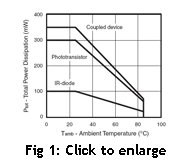
任何半导体设备的动作依靠其模型温度,这就是为什么电子参数要按照特定温度给出。为维持光耦特性,避免失效,通过管理芯片和周围空气之间的热传递限制温度。不应该超过设计规定的连接温度,即使光耦也许没有被归入“功率器件”的种类。这么做有以下两个原因: 首先,全面增加光耦长期可靠性,因为任何固态设备的工作温度都与其长期可靠性成反比。因此应该是器件工作在最低的实际工作温度下。其次,某些参数与设备的问题紧密相连,这些随温度而变得参数包括漏电流、触发电流、CTR、骤回电压和电阻。 进行热计算的三个主要方法是通过使用器件降额值、随温度变化功率图或温度模型。最简单的方法是使用热降额值(假定用功率/度)。然而,制造商非常保守的得到这个数字,所以这个方法不能提供最精确的结果。 随温度变化功率图与第一种方法非常相似,但是用简单的数字代替,依照随温度变化功率图(图1)。并且,这是一个非常保守的方法,应该非常顾及可靠的设计,但是它也不能提供最精确的结果。
进行热计算更全面的方法是使用热模型。一些光耦的热模型已经建立, 英文原文: Thermal characteristics of optocouplers Sustain an optocoupler's performance and avoid failure by managing the heat transfer between the chip and the ambient atmosphere. By Roshanak Aflatouni and Bob Gee, Vishay Intertechnology -- EDN, 10/18/2007 The behavior of any semiconductor device is dependent on the temperature of its die, which is why electrical parameters are given at a specified temperature. To sustain an optocoupler's performance and to avoid failure, the temperature is limited by managing the heat transfer between the chip and the ambient atmosphere. You should not exceed the device's rated junction temperature, even if an optocoupler may not fall into what you consider the "power device" category. This is true for two main reasons. The first is to increase the overall long-term reliability of the optocouplers, as the operating temperature of any solid-state device is inversely proportional to its long-term viability. Consequently, you should operate a device at the lowest practical operating junction temperature. Secondly, certain parameters are closely tied to the operating temperature of the device; these temperature-dependent parameters include leakage current, trigger current, CTR, snapback voltage, and on-resistance. The three main ways of performing thermal calculations are by using a component derating number, or a graph of allowable power versus temperature, or a thermal model. The simplest approach is to use a thermal derating number (given in power/degrees). However, manufacturers are very conservative when deriving this number, so this approach does not provide you with the most accurate results. A graph of allowable power versus temperature is very similar to the first approach, but instead of a simple number, you follow a graph of allowable power versus temperature (Figure 1). Again, this is a very conservative approach and should allow for a very reliable design, but it does not provide you with the most accurate results. A more comprehensive method for performing thermal calculation is to use a thermal model. Thermal models have been created for some optocouplers containing multiple dice ―including phototriacs ― for the most simple and accurate calculations. Multiple Dice Optocoupler Thermal Model This article demonstrates a simplified resistive model. When used correctly, this model produces results that provide "engineering accuracy" for practical thermal calculations. Figure 2 provides the simplified electrical analogous model for any optocoupler. θCA = Thermal resistance, case to ambient, external to the package. θDC = Thermal resistance, detector to case θEC = Thermal resistance, emitter to case θDB = Thermal resistance, detector junction to board θDE = Thermal resistance, detector to emitter die θEB = Thermal resistance, emitter junction to board θBA = Thermal resistance, board to ambient, external to the package TJE = Emitter junction temperature TJD = Detector junction temperature TC = Case temperature (top center) TA = Ambient temperature TB = Board temperature Thermal resistances and specified junction temperatures for a particular device are provided in select datasheets. Thermal Energy Transfer There are three mechanisms by which thermal energy (heat) is transported: conduction, radiation, and convection. Heat conduction is the transfer of heat from warm areas to cooler ones, and effectively occurs by diffusion. Heat radiation (as opposed to particle radiation) is the transfer of internal energy in the form of electromagnetic waves. Heat convection is the transfer of heat from a solid surface to a moving liquid or gas. All three methods occur in optocouplers. However, for most products in most environments, the majority (~ 75 %) This phenomenon is shown graphically in Figures 3a-c by the package temperature profile and strong heat flux contours evident in the die, lead frame, and board via. Because very little heat leaves through the top of the package, the top case temperature is a poor indicator of junction temperature. This means that the majority of the heat is transferred to the board, and very little heat is transferred to the air via the case, which can be verified in the thermal network. Therefore, θDC and θEC can be removed from the thermal model (Figure 2). In this situation, the critical package thermal resistances become θDE, θDB, and θEB. θBA is the thermal resistance from the board to the ambient, and is primarily driven by the geometry and composition of the board. The type of board design used defines this characteristic. Junction-to-case thermal resistances are removed based on the fact that very little heat is leaving through the top of the package (Figure 4). Thermal to Electrical Analogy The thermal-resistance characteristic defines the steady-state temperature difference between two points at a given rate of heat-energy transfer (dissipation) between the points. The temperature difference in a thermal-resistance system in an analog to an electrical circuit, where thermal resistance is equivalent to electrical resistance, is equivalent to the voltage difference, and the rate of heat-energy transfer (dissipation) is equivalent to the current (Table 1). In a thermal circuit, a constant current source represents power dissipation. This is because generated heat must flow (steady-state) from higher temperatures to lower temperatures, regardless of the resi Assuming that you know or can estimate the power dissipated from the detector and the emitter (LED) and the temperature of the board and ambient, you can calculate the node temperatures by solving the network equations. If you desire to use the complete thermal resistance model, a more complex set of network equations will need to be solved. The network equations will provide you with an estimate of what the operating temperature(s) would be before the specific environment is known. As an example, Figure 5 illustrates the analogous electrical model for calculating the temperature at both detector and emitter junctions, given a set of thermal resistances at room temperature with 50 mW on the emitter (PE) and 500 mW on the detector (PD). In order to write an equation to calculate the node temperatures, we will need to assume some heat flow directions (Figure 5). Based on Figure 5, the following equations will calculate the node temperatures: PDE + PDB + PEC = PE (1) - PDE + PDB + PDC = PD (2) TB - TJD + θDB x PDB = 0 (3) TB - TJE + θEB x PEB = 0 (4) TJE - TJD + θDE x PDE = 0 (5) TB - θBA x (PEB + PDB) = TA (6) TC - θCA x (PEC + PDC) = TA (7) TC - TJD + θDC x PDC = 0 (8) TC - TJE + θEC x PEC = 0 (9) Where: PDB = Power dissipation, detector junction to board PDE = Power dissipation, detector to emitter PEB = Power dissipation, emitter junction to board PDC = Power dissipation, detector junction to Case PEC = Power dissipation, emitter junction to Case When the simplified thermal model is used, equations 7-9 do not play any role in the node temperature calculation, and equations 1 and 2 are simplified to equations 1' and 2'. Figure 6a shows a simplified thermal circuit model. Since θCA, θEC, and θDC are not included in the simplified thermal model, all equations that include these resistances (equations 7-9) can be excluded for node temperature calculation. When TA is known, the following equations will calculate the node temperatures: PDE + PDB = PE (1') - PDE + PDB = PD (2') TB - TJD + θDB x PDB = 0 (3) TB - TJE + θEB x PEB = 0 (4) TJE - TJD + θDE x PDE = 0 (5) TB - θBA x (PEB + PDB) = TA (6) For a desired TB and/or when only TB is known, Figure 6a is further simplified (Figure 6b). When TB is given, θBA does not play any role in calculating the node temperature, and any equation(s) that includes θBA can be eliminated. Based on Figure 6, the following equations will calculate the node temperatures when only TB is known: PDE + PDB = PE (1') - PDE + PDB = PD (2') TB - TJD + θDB x PDB = 0 (3) TB - TJE + θEB x PEB = 0 (4) TJE - TJD + θDE x PDE = 0 (5) Example 1: Based on our characterization, Table 2 shows the thermal resistances for a simplified 6-pin dip package optocoupler. As the θBA is dependent upon the material, number of layers, and thickness of the board used, the optocouplers in our analysis were mounted on 2- and 4-layer boards with a thickness of 4 mm. Obviously, the θBA for the two different boards are different (Table 2). Using equations 1'-2' and 3-6, Table 2's thermal resistances, and assuming Figure 6a's emitter and detector power dissipations, Table 3 shows the node temperatures when TA is known. Example 2: You can use the complete thermal model to calculated node temperatures. However, the results would not vary drastically from thermal calculation based on the simplified model for most products and i n most environments. Hence, it is entirely up you to decide how accurate the results are needed for each individual deign. Table 4 provides all thermal resistances for 6-in dip package phototriac.
Using equations 1-9, Table 4's thermal resistances, and assuming Figure 5's emitter and detector power dissipations, Table 5 shows the node temperatures when TA is known. Regardless of the package size and type, the thermal analysis will need to be performed to ensure a solid design. To aid this process, Vishay provides detailed thermal characteristics for newly released optocouplers and solid-state relays (SSRs) that have total power dissipation of 200 mW and higher. This thermal data supplied allows you to more accurately simulate heat distribution and thermal impedance for optocoupler and SSR devices and thus avoid the problems that can arise when thermal parameters are exceeded. |